Architecture to Application of ASIC/VLSI
From conceptualization to final silicon, we provide end-to-end solutions for ASIC and VLSI designs, ensuring efficiency, scalability, and performance in semiconductor applications.
- End-to-End Solutions – Complete support from concept to final silicon.
- Efficiency – Optimized design flow for improved performance.
- Scalability – Flexible solutions to meet future demands.
- High Performance – Designs focused on speed and power efficiency.

Architectural Design
Architectural design defines the system-level structure and behavior of the chip before any detailed logic or physical design begins. This step translates high-level requirements (e.g., speed, power, area, functionality) into a structured plan for the chip’s operation.
- Data path design and control logic planning.
- Defining clock domains and power domains.
- Determines key parameters like throughput, latency, and clock frequency to guide later stages.

IP Development
We focus on custom Intellectual Property (IP) development, designing reusable and optimized hardware IPs that accelerate product development cycles for semiconductor companies.
- Accelerated product development with reusable IPs.
- Enhanced efficiency through optimized hardware IPs.
- Reduced development costs with scalable designs.
- Tailored IPs to meet specific product needs.
- Strategic edge with proprietary IP solutions.

Front End & Back End Design
Front-End Design involves converting architectural specifications into synthesizable RTL code using hardware description languages like Verilog or VHDL.
- Converts RTL into a gate-level netlist using synthesis tools (e.g., Synopsys Design Compiler)
- Constraints like clock frequencies and I/O timing are defined to guide synthesis and optimization.
Back-End Design focuses on the physical realization of the chip – turning the netlist into a layout that can be fabricated.
- Organizing the placement of major blocks on the chip.
- Assigning precise locations to standard cells.

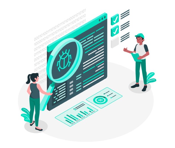
Services: Simulation & Verification
Simulation and verification validate that the RTL (Register Transfer Level) code meets the intended functionality and specifications.
- Checks if the design behaves as expected under all possible input scenarios.
- Performed before synthesis to catch logical errors early.
- Uses tools like ModelSim or VCS to test Verilog/VHDL code.
Product Development
Collaborative Product Development — From Idea to Prototype. Our Product Development services focus on collaborating with clients to turn concepts into working prototypes and product-ready solutions. Rather than complete silicon delivery, we provide specialized design expertise to strengthen your product journey.
- System-level design and architecture support.
- Integration of custom and third-party IPs into products.
- Rapid prototyping and proof-of-concept development.
- Hardware-software co-design support for specific applications
- Focus on quality, performance, and faster time-to-market.

Establishing Prototype Foundry
We aim to set up a dedicated prototype foundry, enabling rapid prototyping and small-scale manufacturing, accelerating semiconductor R&D in India.
- Rapid Prototyping – Faster turnaround for design validation.
- Small-Scale Manufacturing – Cost-effective production for early-stage designs.
- Accelerated R&D – Reduced development costs with scalable designs.
- Local Capability – Strengthening India’s semiconductor ecosystem.
- Innovation Hub – Facilitating experimentation and design improvements.

Saptarshi Academy
Empowering future engineers and professionals through specialized VLSI and Semiconductor courses. Saptarshi Academy offers hands-on training in ASIC, FPGA, Design Verification, and Embedded Systems, bridging the gap between academia and industry.
- Industry-Relevant Skills
Curriculum designed to match industry standards and requirements. - Hands-On Experience
Practical training in ASIC, FPGA, Design Verification, and Embedded Systems. - Expert Guidance
Learn from experienced industry professionals. - Career Readiness
Develop job-ready skills for the semiconductor and VLSI industry.